- About this module
- What is a memory device?
- SR Latch
- D-flipflop
- Edge sensitive D-flipflop
- Clocked and gated D=flipflop
- One last detail
- Multi-bit registers
About this module
-
Prerequisites: Module 0281
-
Objectives: This module explores the most basic memory devices implemented in logic gates, including the flexible D-flipflop.
What is a memory device?
A logic gate is not a memory device because the state of the output changes as the inputs change. A memory device has a guarded internal state that remains unchanged until a specific input pattern triggers the change.
SR Latch
A “latch” is a basic memory device because its state is latched unless there is an explicit signal to change the state. Let us examine the basic logic design of an SR-latch.
Instead of using a diagram to represent the logic design, let us use an alternative description. In this description language, we borrow ideas from C/C++ programming, but we also add some unique elements so that it is useful in circuit description.
First, we can see gate types as classes. For example, Nand2 refers
to the class describing the properties and behavior of a nand2 gate.
Let’s see whether the following description works:
Nand2 n1, n2;
InputPin s, r;
OutputPin q, nq;
circuit.addNode(new Node(s.pin, n1.in[0]));
circuit.addNode(new Node(r.pin, n2.in[1]));
circuit.addNode(new Node(n1.out, n2.in[0], q.pin));
circuit.addNode(new Node(n2.out, n1.in[1], nq.pin));
A “node” in a circuit diagram represents a logical electrical connection. A node connects “ports” of circuit components. In the above description, “n1” and “n2” are nand2 gates. “s” and “r” are input pins, “q” and “nq” are output pins.
Our first exercise is to draw a diagram of this circuit.
Once the diagram is drawn, you may notice that this circuit is different from most of the other circuits like adders and subtractors. A carry-lookahead adder may be complex, but it has no “loops”!
The loop nature of an SR latch is exactly the reason why it is a basic memory device. The output states feed back to the input state to reinforce/maintain the state of the device. This allows the circuit to ignore certain input states while maintaining the output states.
Let us start our analysis of this circuit with input states that guarantee some output states:
-
s.state = 0{.c} makess.pin == 0{.c}. Sinces.pinconnects ton1.in[0],n1.outbecomes 1. -
r.state = 0makesr.pin == 0. Sincer.pinconnects ton2.in[1],n2.outbecomes 1.
Now let us examine the following sequence of state changes:
-
s.state = r.state = 0: this sets both output pins to 1. -
r.state = 1: becauses.pin == 0,n1.out == n2.in[0] == 1. Combined withr.pin == n2.in[1] == 1,nq.state == 0. -
s.state = 1: becausen2.out == n1.in[1] == 0at this point, even ifs.pin == n1.in[0] == 1,n1.out == 1.
Now compare to this sequence of input pin state changes:
-
s.state = r.state = 0 -
s.state = 1 -
r.state = 1
By reversing the ordering of letting the input pins return to 1, the
output of the device is different! This is despite in both sequences we
end up with s.state == r.state == 1. The ability of an SR latch to be
able to latch to different output states despite the same input states
has to do with the feedback mechanism so that the output states form an
internal feedback to the input to maintain certain output states.
This means the truth table of an SR latch is a bit trickier than other circuits:
| s | r | q | nq |
|---|---|---|---|
| 0 | 0 | 1 | 1 |
| 0 | 1 | 1 | 0 |
| 1 | 0 | 0 | 1 |
| 1 | 1 | NC | NC |
The last row of the truth table says “q and nq maintain their original states, no change (NC)”.
The names of the devices are significant. “s” means “set”, “r” means “reset”. “q” is the main output of an SR latch, “nq” is basically “not q”, the negated output.
You may also notice that “s” is an “active low” signal. This means that when the signal is low (0), it sets “q”. This is why oftentimes “s” as a pin is also written as “/s” where the slash symbol represents negation. The same applies to “r”.
While being crude, an SR latch is a memory device because of its ability to remember its state when both inputs are 1. As a result, SR latches form the foundation of more complex and flexible memory devices.
Let us conclude this section by defining the ports of a SR-Latch:
-
SRLatch.s: the active low input to set the latch. -
SRLatch.r: the active low input to reset the latch. -
SRLatch.q: the output/state of the latch. -
SRLatch.nq: the negated output/state of the latch.
An interesting question is what if the input of an SR latch changes from
s==r==0 to s==r==1 simultaneously?
Because a real NAND2 device has a latency and does not respond to input changes simultaneously, there is a delay from the time the input experiences a change to the output reflecting the change. Let us assume “n1” has a latency of $t_1$ while “n2” has a latency of $t_2$. The overall time is $t$. For this discussion, assume $t_1 < t_2$.
-
at time $t=0$, both
n1,in[0]andn2,in[1]transition from 0 to 1. -
at time $t=t_1$,
n1.out == 0responding to the event at time $t=0$. -
at time $t=t_2$,
n2.out == 0responding to the event at time $t=0$. -
at time $t=t_2+t_1$,
n1.out == 1responding to the event at time $t=t_2$, but at the same time,n2.out ==1responding to the event at time $t=t_1$. -
back to the first step!
’
This is called an oscillation!
D-flipflop
A D-flipflop is a memory device that is built on top of an SR-latch. Unlike an SR-latch, a D-flipflop has a data bit (hence the name D) that specifies the value to store (1 or 0), and a separate “clock” that serves as the enabler to change the state of the SR-latch.
The following is the text description of a D-flipflop:
Not n;
Nand2 n1, n2;
SRLatch sr;
InputPin d, en;
OutputPin q,nq;
circuit.addNode(new Node(d.pin, n1.in[0], n.in));
circuit.addNode(new Node(en.pin, n1.in[1], n2.in[0]));
circuit.addNode(new Node(n.out, n2.in[1]));
circuit.addNode(new Node(n1.out, sr.s));
circuit.addNode(new Node(n2.out, sr.r));
circuit.addNode(new Node(sr.q, q.pin));
circuit.addNode(new Node(sr.nq, nq.pin));
Because “en” connects to both “n1” and “n2” (the NAND2 gates), when “en”
is a 0 (not enabled), the outputs of “n1” and “n2” guarantee to be 1’s.
From the SR-latch discussion, having both inputs to an SR latch being
1’s maintain the current state. This is why “en” is called the “enable”
pin. When en.state == 0, the SR-latch “sr” just maintains its state.
When “en” is 1, however, then the actual output of “n1” and “n2” is decided by the other input of each of the NAND2 gates. The other input to the NAND2 gates are the “data” and the negation of the “data”. This means exactly one of the NAND2 gates outputs a 1 and other one outputs a
- The one that outputs a 0 (because both inputs are 1s) alters the state of the SR-latch accordingly.
The key feature of a D-flipflop is that an input port is dedicated to specifying the new state of the memory unit, whereas the other input port is dedicated to enable/disable the update. This means a bank of D-flipflops can be used to store multiple bits sharing the same enable.
Edge sensitive D-flipflop
The design in section D-flipfop is “level sensitive” because the state of the SR latch keeps updating according to the data port as long as the enable port is a 1. This is often not desirable in a practical design where multiple memory devices share the same data nodes.
An edge-sensitive design updates at the exact moment of the transition of a “clock” or “clk” port. The “edge” is a transition from 0 to 1 or a transition from 1 to 0. Most designs are sensitive only to one edge (rising edge 0 to 1, or falling edge 1 to 0).
The following is the design of a positive-edge sensitive D-flipflop:
SRLatch s, c;
Nand3 n1;
Nand2 n2
InputPin clk;
InputPin data;
OutputPin q;
circuit.addNode(new Node(data.pin, n2.in[1]));
circuit.addNode(new Node(clk.pin, s.r, n1.in[1]));
circuit.addNode(new Node(n2.out, n1.in[2], s.s));
circuit.addNode(new Node(n1.out, n2.in[0], c.r));
circuit.addNode(new Node(s.nq, n1.in[0],c.s));
circuit.addNode(new Node(c.q, q.pin));
Again, a good exercise is to draw the actual design in a circuit diagram.
This design is a little more difficult to analyze because the key is the transition of clk from 0 to 1.
The analysis is divided into several sections.
data=0 clock rising edge
-
clk.pin == 0, data.pin == 0:-
s.r == 0, causings.nq == c.s == 1. -
n1.in[1] == 0, causingn1.out == c.r == 1 -
SR latch “c” maintains its state
-
-
clk.pin == 1, data.pin == 0:-
s.s == 1, s.r == 1, therefores.nq == c.s == 1is maintained. -
n1.[0] == s.nq == 1,n1.[1] == 1,n1.[2] == n2.out == 1, thereforen1.out == c.r == 0, this causesc.q == 0, c.nq == 1
-
data=1 clock rising edge
-
clk.pin == 0, data.pin == 1:-
s.r == 0, causings.nq == c.s == 1. -
n1.in[1] == 0, causingn1.out == c.r == 1 -
SR latch “c” maintains its state
-
-
clk.pin == 1, data.pin == 1:-
n2.out == n1.in[2] == 0, thereforen1.out == c.r == 1. We know SR latch “c” is not resetting. -
s.s == n2.out == 0, as a result,s.nq == c.s == 0, this causes the SR latch “c” to turn on, resulting inc.q == 1
-
clk steady state insensitivity
It is fairly clear that when clk.pin == 0, c.s == c.r == 1, which
means the value of data.pin has no impact to the system.
However, we also have to show that when clk.pin == 1, transitions of
data.pin does not affect the output of the SR latch “c”.
To perform this analysis, we start with the clk.pin == 1 state of the
previous section.
After a rising clock edge when data.pin == 0:
-
clk.pin == 1, data.pin == 0:-
s.s == 1, s.r == 1, therefores.nq == c.s == 1is maintained. -
n1.[0] == s.nq == 1,n1.[1] == 1,n1.[2] == n2.out == 1, thereforen1.out == n2.in[0] == c.r == 0, this causesc.q == 0, c.nq == 1
-
-
clk.pin == 1, data.pin == 1:-
n2.in[1] == 1, however, sincen1.out == n2.in[0] == 0from the previous state,n2.out == 1continues -
there is no further change to the rest of the circuit
-
After a rising clock edge when data.pin == 1:
-
clk.pin == 1, data.pin == 1:-
n2.out == n1.in[2] == 0, thereforen1.out == c.r == 1. We know SR latch “c” is not resetting. -
s.s == n2.out == 0, as a result,s.nq == c.s == 0, this causes the SR latch “c” to turn on, resulting inc.q == 1
-
-
clk.pin == 1, data.pin == 0:-
n1.out == n2.in[0]==1from the previous state, combined withdata.pin ==0, this results inn2.out == 1. This is a transition. -
s.s == n2.out == 1. This alone has no effect. -
n1.in[2] == n2.out == 1, but this also has no effect because from the previous state,s.nq == n1.in[0] == 0, as a result we maintainn1.out == 1. -
because
s.nq == 0andn1.out ==1are maintained, the SR latch “c” remains unchanged (continue to be in a on state).
-
The above analysis concludes that after a rising clock edge triggering
potentially a change, as clk.pin == 1, data.pin can change without
affecting the state of the SR latch “c”. As a result, we show that the
device is data insensitive when clk.pin == 1.
Clocked and gated D=flipflop
This design is getting a little tedious to describe using text! Here is the actual image:
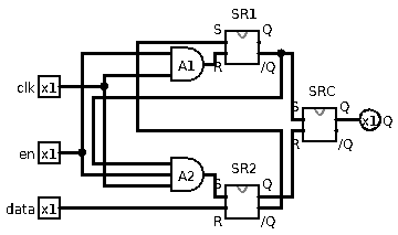
(clk is “when”, en is “who” and data is “what”)
This design is built based on a clocked D-flipflop. SR2 is really
mostly in the previous clocked D-flipflop, except one of the NAND gates
had 3 inputs instead of 2. This is accomplished by using a standard SR
latch, but with one of the inputs further gated by a 2-input AND gate.
The 3rd input is handled internally inside the SR latch.
The gated and clocked D-flipflop is different only in the sense that
SR1.R is further gated by en.pin. This means that when
en.pin == 0, A1.out == 0 regardless of the other input of A1. As
a result, SR1.nq is guaranteed a 1. However, this one is connected to
SRC.S, recall that SRC.S == 1 means we are not setting because this
input is active low.
The same applies to en.pin connected to A2, eventually making
en.pin == 1 causing SRC.S == 1 and SRC.R == 1, all without caring
the other two input pins. An SR latch that has both inputs being 1
simply maintains its state.,
This gated and clocked D-flipflop has several advantages. First, being
gated means its update can be disabled by en.pin == 0. This is very
helpful in a circuit where data nodes are multi-dropped. The clocked
nature is also useful to synchronize the update of multiple memory units
in the same instant.
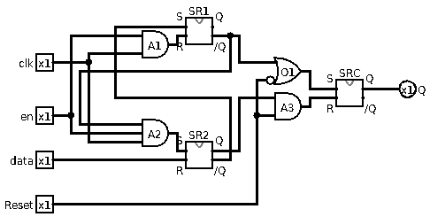
One last detail
When a computer powers up, some states of the gates are unknown. As a result, it is helpful to have a global reset signal to reset everything to a known state.
By gating the inputs of SRC with an active low reset.pin, the
content of a D-flipflop can be reset to 0 during the start-up phase of a
computer. The resulting circuit is as follows:
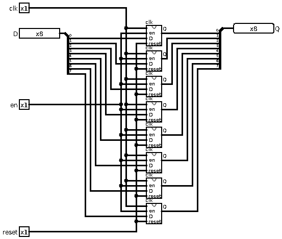
Multi-bit registers
A multi-bit register is, in a way, like a multi-bit gated and clocked D-flipflop.