About this module
-
Prerequisites: 0298
-
Objectives: This module discusses how simple clocked circuits work.
Registers
A “register” is a multi-bit, usually resettable, usually gated, and usually edge-sensitive D-flipflop. A register usually has the following ports (interfaces):
-
Data: The D port serves as a multi-bit input port so that new content can be specified. Upon presentation of new data, however, a register does not update immediately.
-
clock: the clk port is edge sensitive, we assume it is rising edge sensitive. A register only updates when the edge occurs. This is important because it limits the actual update to a very short window when the D port has a valid date.
-
enable: the en port is level sensitive and “gates” a register In a processor, many registers often share the same system-wide clock signal and data bus. The en port allows a single bit be used to designate which register be overwritten.
-
reset, also called clear: this port is active low. When asserted (low), a register resets its value to 0.
-
Q: this is the multi-bit output port, it always presents the current value of the register.
Though somewhat complex compared to an SR latch and simpler D-flipflops, a register is still considered fairly simple and therefore fast. Registers can keep up with computational circuits like adders and subtractors.
Synchronizing operations
Every component of a processor has a latency, measured as the time between the input signals presented and the output signals reflecting the operation of the component. For instance, a 3-bit carry-lookahead adder has a latency delay that is equivalent to 5 times the latency delay of a simple gate (AND, OR, XOR).
As a result, it is important to have a basic beat to provide a system wide time base for all components in a processor. This time base is often called the system clock or simply the clock.
The clock signal is often a fixed-frequency square wave. The edges of a a clock signal is like the drum or bass beat of the music, providing a timing mechanism for all the components.
Not all components of a processor are “clocked”. A clocked component is one that updates or performs an operation when the clock input transitions (from low to high, or from high to low). For example, an adder or a subtractor is not clocked. Such circuits stars to respond to input changes as soon as the changes occur.
On the other hand, components like registers are clocked. This means that the input signal of a register can change arbitrarily. Unless the clock input has a transition, all changes to the other input ports are ignored and the internal state of a register is not altered.
Example
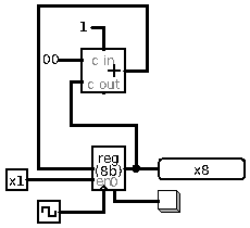
This is a circuit that increments the value of the register when the clock ticks.
Note how the adder is “always” outputting a value that is one more than the output of the register. “Always” is quoted because there is a slight latency between the input of the adder changing and the output of the adder reflecting that change. In return, the output of the adder is connected to the input of the register.
The key to this design is the clock signal. While the simulator allows the clock to be clicked manually. In a real computer, however, the clock signal keeps ticking. This can also be emulated in Logisim.
The update of the register is gated by the enable (EN) port. Once enabled, the register only updates when there is a rising edge at the clock port. This permits the register to increment, but only once. After the rising edge, despite the adder presenting a number that is one more than the output of the register itself, the register does not update due to its edge sensitivity.